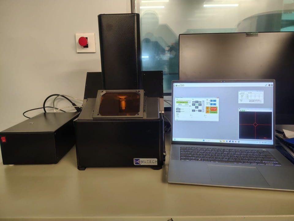
Direct Laser Lithography System
Model: µLaser | Manufacturer: Mutech Microsystems (Argentina)
| Overview
The µLaser by Mutech Microsystems is a direct laser lithography writer designed for microfabrication research and prototyping. Using a precision 405 nm laser and industry-standard optics, it patterns photosensitive resist at high resolution across large areas, enabling in-house creation of photomasks, micro-devices, and research prototypes.
| Key Features
Fabrication Technology
Direct laser lithography using a focused 405 nm diode laser – µLaser writes directly on photoresist without masks, reducing fabrication time and costs. Direct lithography enables versatile prototyping from photomasks to functional microstructures.
Laser Source
405 nm diode laser (optionally 375 nm) – The UV laser source offers fine energy deposition suitable for high-resolution patterning. An optional 375 nm source expands compatibility with additional resist chemistries.
Minimum Feature Size
3-5 µm realistic feature capability – Minimum feature sizes vary with optics and substrate, enabling fine micro-patterning. This resolution suits microfluidics, MEMS,
and basic microelectronics prototyping.
Writing Area
Up to 100 × 92 mm² large writing field – The generous write area supports full-size photomask patterning or large microstructures. It enables broad substrate coverage without stitching or repositioning.
Positioning & Stage
High-precision XY motion with nm-level steps – The stage offers unidirectional steps of X = 0.16 µm and Y = 1.00 µm for fine control. Multi-layer alignment accuracy can be improved with an optional rotary stage (5-10 µm).
Optics & Focusing
Confocal microscope with integrated camera and yellow illumination – Microscope optics ensure accurate focusing and alignment before writing. Industry standard objectives allow spot size adjustment for different resolutions.
Software & File Support
User-friendly control with PNG and GDSII import – Software supports design transformations including rotation, reflection, scaling, and borders. It enables multi-design printing and compensates for substrate tilt/curvature.
Writing Speed & Modes
100-120 mm/s typical writing speed – Combined with multiple optics, this enables efficient throughput on large areas. Supports both unidirectional and bidirectiona writing for optimized patterns.
Applications
Photomask fabrication, research prototype patterning, microfluidics, microelectronics, micromechanics, sensor structures, and material science research. Ideal for universities and R&D facilities developing custom microdevices and prototypes. The integrated vision and alignment system simplifies pattern registration on pre-existing features.